(Hong Kong)

Product Summary
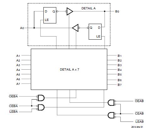
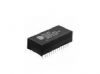
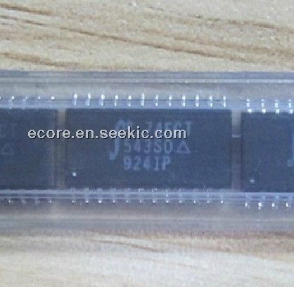
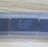
The 74FCT543SO is a non-inverting octal transceiver built using an advanced dual metal CMOS technology. The 74FCT543SO contains two sets of eight D-type latches with separate input and output controls for each set. For data flow from A to B, for example, the A-to-B Enable (CEAB) input must be LOW in order to enter data from A0–A7 or to take data from B0–B7, as indicated in the Function Table. With CEAB LOW, a LOW signal on the A-to-B Latch Enable (LEAB) input makes the A-to-B latches transparent; a subsequent LOW-to-HIGH transition of the LEAB signal puts the A latches in the storage mode and their outputs no longer change with the A inputs.
Parametrics
74FCT543SO absolute maximum ratings: (1)VTERM Terminal Voltage with Respect to GND: -0.5 to +7.0V; (2)VTERM, Terminal Voltage with Respect to GND: -0.5 to VCCV; (3)TA, Operating Temperature: 0 to +70℃; (4)TBIAS, Temperature Under Bias: -55 to +125℃; (5)TSTG, Storage Temperature: -55 to +125℃; (6)PT, Power Dissipation: 0.5W; (7)IOUT, DC Output Current: 120mA.
Features
74FCT543SO features: (1)IDT54/74FCT543 equivalent to FAST speed; (2)IDT54/74FCT543A 25% faster than FAST; (3)IDT54/74FCT543C 40% faster than FAST; (4)Equivalent to FAST output drive over full temperature and voltage supply extremes; (5)IOL = 64mA (commercial), 48mA (military); (6)Separate controls for data flow in each direction; (7)Back-to-back latches for storage; (8)CMOS power levels (1mW typ. static); (9)Substantially lower input current levels than FAST (5mA max.); (10)TTL input and output level compatible; (11)CMOS output level compatible; (12)Product available in Radiation Tolerant and Radiation Enhanced versions; (13)Military product compliant to MIL-STD-883, Class B.
Diagrams