(Hong Kong)

Product Summary
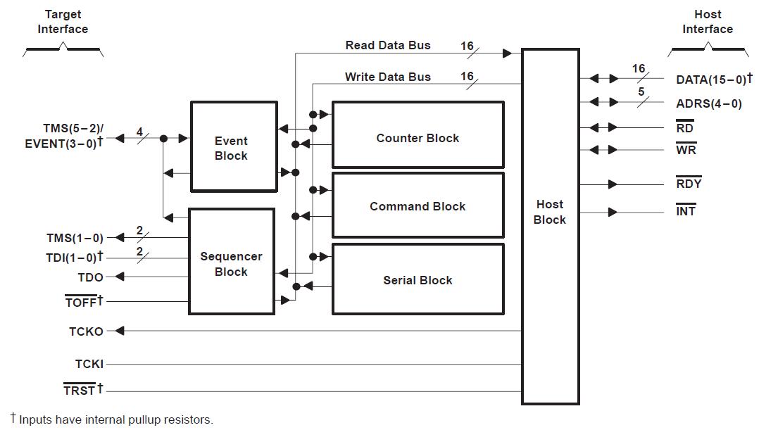
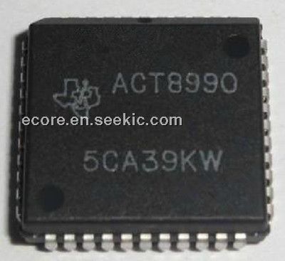
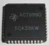
The ACT8990 is a test-bus controller (TBC). The ACT8990 is a member of the Texas Instruments SCOPEE testability integrated-circuit family. This family of components supports IEEE Standard 1149.1-1990 (JTAG) boundary scan to facilitate testing of complex circuit-board assemblies. The ACT8990 differs from other SCOPEE integrated circuits. Their function is to control the JTAG serial-test bus rather than being target boundary-scannable devices. The required signals of the JTAG serial-test bus-test clock (TCK), test mode select (TMS), test data input (TDI), and test data output (TDO) can be connected from the TBC to a target device without additional logic.
Parametrics
ACT8990 absolute maximum ratings: (1)Supply voltage range, VCC: -0.5 V to 7 V; (2)Input voltage range, VI (see Note 1): -0.5 V to VCC; (3)Output voltage range, VO (see Note 1): -0.5 V to VCC; (4)Input clamp current, IIK (VI < 0 or VI > VCC): ±20 mA; (5)Output clamp current, IOK (VO < 0 or VO > VCC): ±20 mA; (6)Continuous output current, IO (VO = 0 to VCC): ±25 mA; (7)Maximum power dissipation at TA = 55℃ (in still air) (see Note 2): FN package: 1.5W; (8)Storage temperature range, Tstg: -65℃ to 150℃.
Features
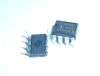
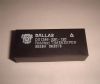
ACT8990 features: (1)Members of the Texas Instruments SCOPE Family of Testability Products; (2)Compatible With the IEEE Standard 1149.1-1990 (JTAG) Test Access Port and Boundary-Scan Architecture; (3)Control Operation of Up to Six Parallel Target Scan Paths; (4)Accommodate Pipeline Delay to Target of Up to 31 Clock Cycles; (5)Scan Data Up to 232 Clock Cycles; (6)Execute Instructions for Up to 232 Clock Cycles; (7)Each Device Includes Four Bidirectional Event Pins for Additional Test Capability; (8)Inputs Are TTL-Voltage Compatible; (9)EPIC E (Enhanced-Performance Implanted CMOS) 1-mm Process; (10)Packaged in 44-Pin Plastic Leaded Chip Carrier (FN), 68-Pin Ceramic Pin Grid Array (GB), and 68-Pin Ceramic Quad Flat Packages (HV).
Diagrams